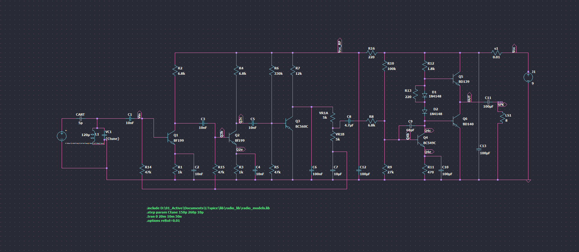
← Back to Evan Systems

Radio Project

Discrete Transistor AM Radio Receiver

Physical build, LTspice simulation, and interactive schematic explorer for a discrete transistor AM receiver.

9 V battery powered Discrete BJT signal chain 1 MHz AM simulation 8 Ω speaker load

Overview

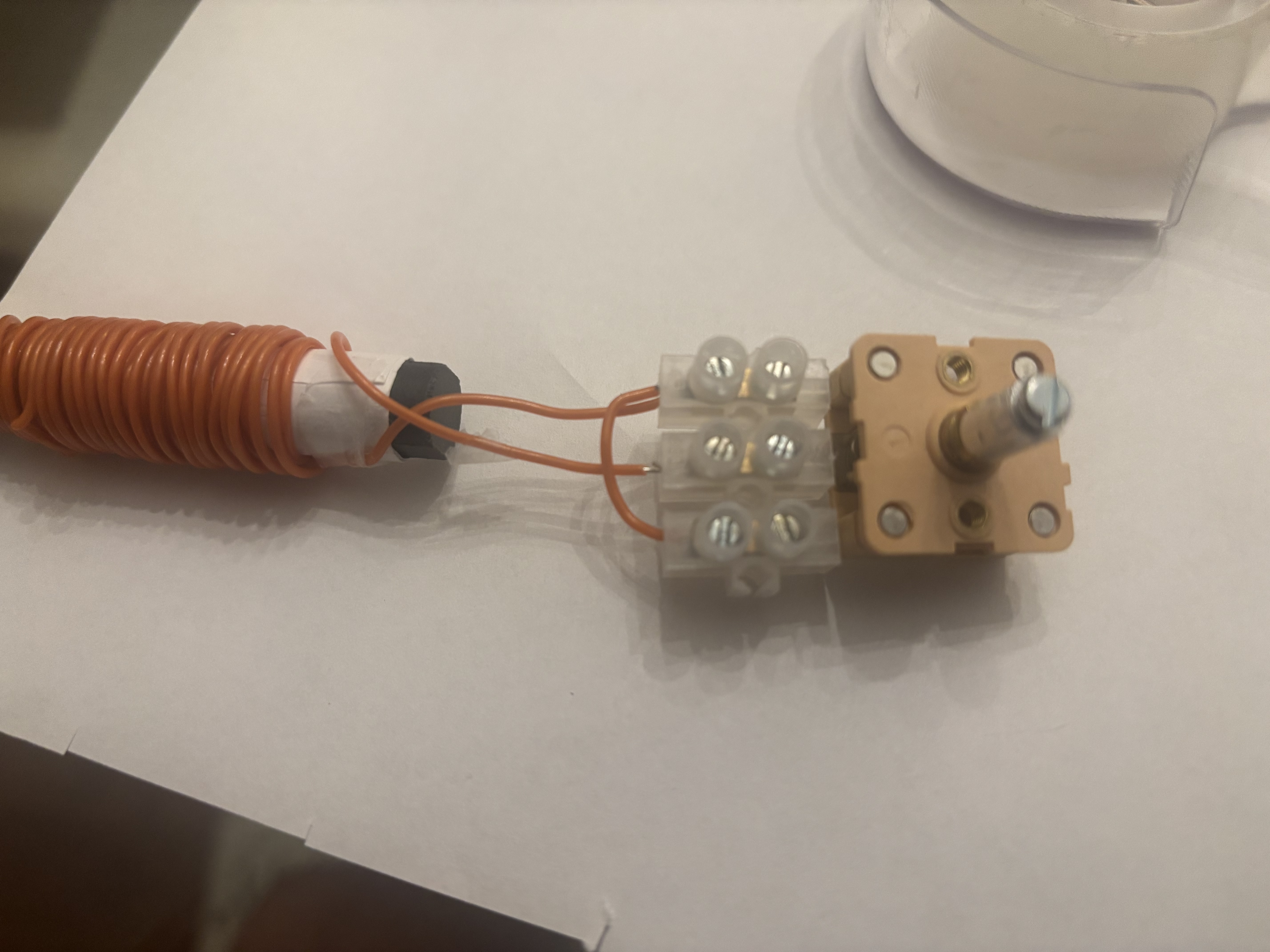
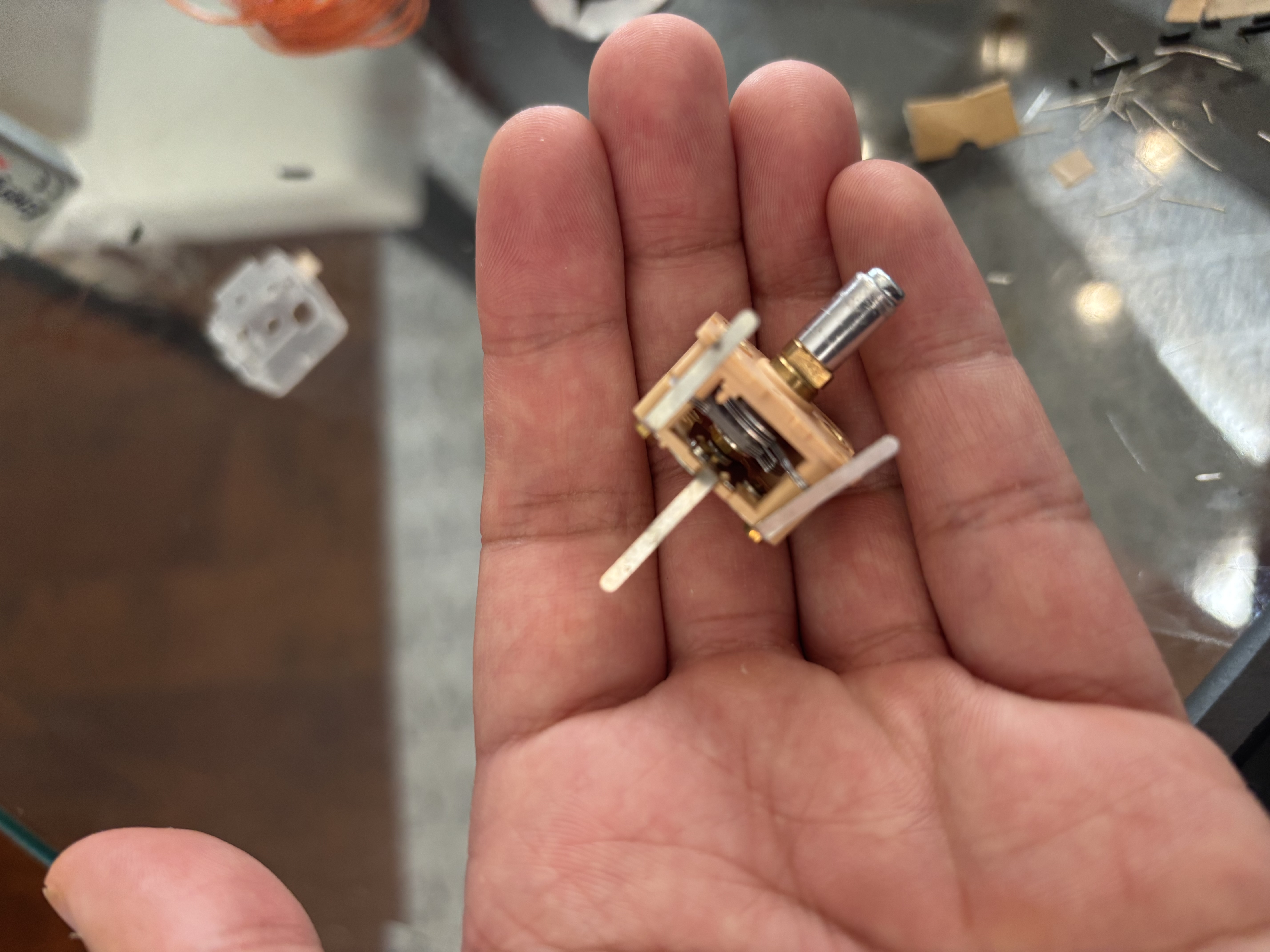
This project is a 9 V battery-powered AM radio receiver built around discrete transistor stages rather than an integrated radio IC. The page documents the physical antenna and tuning build, the LTspice model, and the signal path from RF pickup through audio output.

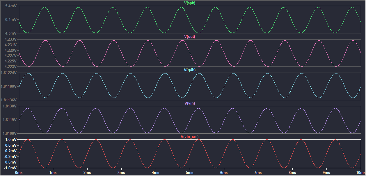
The receiver is modeled as a tuned LC front end followed by RF gain, detection and preamp control, and a complementary transistor audio output stage driving a speaker load. This first version focuses on what each block does, how it was approximated in simulation, and what still needs to be measured against the physical build.

Power9 V battery supply
Tuned inputL1 = 120 µH with VC1 swept near resonance
Source1 MHz carrier amplitude-modulated by 1 kHz tone
Output loadSpeaker represented as 8 Ω in LTspice

Physical Build

The physical front end uses a hand-wound coil on a ferrite rod and a mechanical variable capacitor for tuning. Moving the capacitor changes the resonant point of the LC tank and determines which part of the AM band is emphasized before amplification.

Ferrite rod coil connected to terminal block and variable capacitor
Ferrite rod coil and tuning capacitor connection hardware.
Small mechanical variable capacitor held in hand
Mechanical variable capacitor used for tuning experiments.
Build note: the simulation treats the ferrite antenna as a lumped inductor so the first-order tuning behavior can be studied before adding parasitics, coil loss, coupling, and antenna geometry.

Signal Chain

The receiver is divided into layered functional blocks. Each layer has a simple job: select the station, increase RF level, extract the audio envelope, control the audio level, and drive the speaker.

LC tankL1 + VC1 select the carrier
Q1First RF transistor stage
Q2Second RF transistor stage
Q3 + VR1Detector / preamp and level control
Q4Audio driver
BD139 / BD140Push-pull output stage
8 Ω speakerModeled as resistor load

Circuit Overview

The schematic is treated as a set of layers instead of one large mystery circuit. Open each block below to inspect the role of that part of the receiver.

LTspice schematic of the discrete transistor AM radio receiver
LTspice schematic for the full discrete AM receiver model.
Input tuning: LC tank

The front end uses L1 = 120 µH and VC1 swept around resonance. This approximates the ferrite rod and variable capacitor combination used in the physical receiver.

RF path: Q1 → Q2

Q1 and Q2 provide transistor RF gain after the tuned input. In the simulation, these stages help show how the selected carrier is passed forward before envelope recovery.

Detector / preamp: Q3 + VR1

Q3 and VR1 form the detector/preamp control layer. This is where the AM envelope becomes the useful low-frequency audio signal and where level adjustment is introduced.

Audio output: Q4 → BD139/BD140

Q4 drives the complementary BD139/BD140 output stage. The output is coupled into an 8 Ω speaker load, represented as a resistor in LTspice for a first-pass simulation.

LTspice Simulation Setup

The LTspice source is configured as a controlled AM test signal rather than a real antenna environment. A 1 MHz carrier is amplitude-modulated by a 1 kHz tone, making it easier to verify that the receiver passes RF energy and recovers the audio envelope.

Modeled conditions

  • 9 V DC supply, matching the battery-powered build target.
  • Ferrite rod represented as a lumped 120 µH inductor.
  • Variable capacitor swept around resonance to demonstrate tuning selectivity.
  • Speaker represented as an 8 Ω resistor load.

Simulation focus

  • Confirm the LC tank tuning point.
  • Observe signal transfer through Q1 and Q2.
  • Inspect recovered 1 kHz audio behavior.
  • Compare output stage behavior under an 8 Ω load.
.step param Ctune 150p 260p 10p
.tran 0 20m 10m 50n
.options reltol=0.01

Results

The first simulation pass shows the expected low-frequency audio tone appearing at later nodes and at the speaker load after the RF and detector stages. The variable capacitor sweep gives a way to compare response near resonance and verify that tuning has a measurable effect.

LTspice waveform viewer showing recovered audio and output signals
Example LTspice waveforms showing source, internal nodes, output, and speaker load response.
Recovered audio1 kHz behavior is visible after detection and audio amplification.
Tuning selectivityVC1 sweep demonstrates how resonance changes the receiver response.
Load checkThe BD139/BD140 output layer is tested against an 8 Ω speaker approximation.

Debugging Process

The debugging plan follows the same layered structure as the page: prove each block before blaming the whole receiver. The most useful checks are node-by-node comparisons between the physical build and the LTspice model.

  1. Start at the LC tank: verify continuity, tuning capacitor range, and approximate resonant behavior.
  2. Check transistor bias: confirm each transistor is biased into the intended operating region before tracing signals.
  3. Inject known signals: use the simulated 1 MHz AM source as a reference for bench testing where possible.
  4. Trace stage outputs: compare Q1, Q2, detector/preamp, and speaker-node behavior against the simulation.
  5. Separate RF and audio faults: determine whether a failure occurs before detection or after the audio driver/output stage.

Modeling Assumptions and Limitations

This simulation is intentionally simplified so the circuit layers can be understood and tuned quickly. The assumptions are useful for a first pass, but they also define where the model may differ from the hardware.

Assumptions

  • Ferrite rod is approximated as a lumped inductor.
  • Speaker is approximated as a fixed 8 Ω resistor.
  • AM input is an ideal 1 MHz carrier with 1 kHz modulation.
  • Variable capacitor sweep represents tuning selectivity.

Limitations

  • Ferrite coupling, orientation, Q, and winding parasitics are not fully modeled.
  • Real speaker impedance varies with frequency and enclosure conditions.
  • Transistor model tolerances may not match the exact physical parts.
  • External station strength, noise, grounding, and hand capacitance are excluded.

Files / Next Steps

This first portfolio version documents the architecture and simulation approach. The next version can add downloadable LTspice files, measured bench results, and a deeper schematic walkthrough as the physical build is refined.

Files to add
  • LTspice schematic and model library download.
  • Bill of materials for transistor, coil, capacitor, and output-stage parts.
  • Bench measurement screenshots or oscilloscope captures.
Next steps
  • Measure real LC resonance and compare against the 120 µH approximation.
  • Characterize tuning range across the variable capacitor travel.
  • Replace the 8 Ω resistor model with a more realistic speaker impedance model.
  • Add a lightweight schematic explorer overlay after the page content is finalized.